Markets
Futurrex is enabling the evolution of microfabrication.
For decades companies have been using similar chemistries from traditional providers resulting in ever-more commoditized physical properties which spurred mass volume production in the microelectronics and related industries.
Eventual commoditization across chemistries has resulted in diminishing differentiation for the end customer product however.
Today using novel chemistries, unique and more simplified processing techniques with proprietary processing methods, Futurrex’s solutions are enabling the fastest growing, next generation markets that will shape the next 20 years:
- MEMS,
- energy efficient lighting,
- alternative energy generation,
- communications components,
- display technologies,
- biotechnology and
- packaging solutions.
Engineering teams are working globally with Futurrex’s chemistries and technical oversight on exciting breakthroughs that will create the next killer application in a variety of markets.
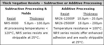
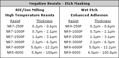
The unique physics displayed by our products facilitates larger processing windows, higher thicknesses, higher temperatures, better adhesion, simpler processing and faster throughput at lower cost.
In some cases, entire lines of capital equipment can be completely avoided in the production of semiconductor components.
Today there is no reason that customer end products should not differentiate themselves not only in design but in core physical characteristics.
Whether a customer chooses a custom-designed chemistry specific to them or a long-standing core product line, Futurrex ensures success throughout prototyping, technology transfer, volume manufacturing and reliable scaling beyond the first production facility. Our philosophy of partnering with each customer to optimize their process allows customers to further differentiate their product performance in every parameter important to them. No other company will provide you with a quick, exact custom-made solution for your engineering task or a clever, cost-efficient process based on one of the core product suites we provide.
Whether a customer needs an enabling technology or a solution with fast ROI, Futurrex has the turnkey productivity tools to enable an engineer quick testing, prototyping and product development with a reliable supply chain.
Please inquire within and do not hesitate to see what we can do for your application or market.
